
With the world more dependant than ever on technological innovations for the continual function of society, companies like NEO SEMICONDUCTOR are becoming more of a cornerstone than ever before in these efforts. As the exponential curve of innovation keeps rising, and 5G and AI technologies become more widespread, organisations will find themselves in need of ensuring that other elements of their system can work in tandem with such systems in order to allow them to truly benefit from their full capacity. Thus, NEO SEMICONDUCTOR has earned itself the title of the ‘Most Innovative Flash Memory Startup Company’ for 2020 in California by serving this need, providing a new and better flash memory solution for a new epoch.
NEO SEMICONDUCTOR, the winner of the most innovative flash memory startup award for 2020, has been making a name for itself with its ‘Best in Show’ product. Fundamentally, this company has been making waves since its inception, with this coming to a head during the Flash Memory Summit Conference in November of 2020; during this show, NEO SEMICONDUCTOR displayed its breakthroughs in 3D NAND Flash Memory and Architecture to a wowed crowd that went on to spread the word amongst further facets of the industry. 3D NAND flash memory, in essence, can be described as the main data storage facilitation unit used in smart phones, solid state drives, cloud storage facilities, data centres, USB drives, IoT devices, drones, and AI robotic technologies.
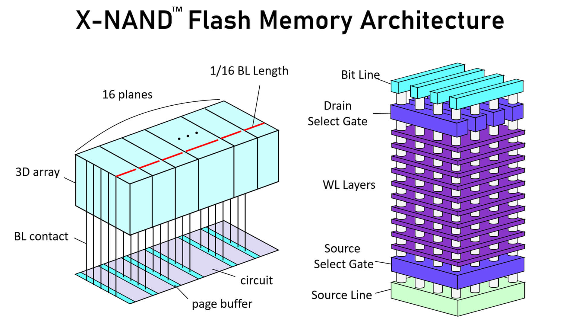
X-NAND, therefore, is a revolutionary new version of this that aids the operations intrinsic to each of these systems working effectively. A revolutionary new way to think about 3D NAND flash memory architecture, X-NAND provides 3 times faster speed and more than 10 times the data throughput than conventional NAND flash, without an increase in cost or footprint bogging it down. In essence, it is a streamlined, relatively wasteless, and elegant solution, rejecting additional bloatware for a speedier, more cost-efficient experience that 5G, AI, and many other applications can incorporate easily and to great effect.
NEO SEMICONDUCTOR promises that a client will be able to benefit from the changes that switching to X-NAND can make from day one. With a variety of top-of-the-range features that have been implemented in order to make X-NAND’s advantages over regular NAND abundantly plain, the elements that set it apart come down the architecture of the structure itself. Essentially, whilst the traditional 3D NAND flash memory device only have 2-4 planes in the Y-direction, X-NAND can increase the number of planes by order of magnitude, even reaching numbers of between 16 and 64 without ever increasing the size of the chip proper, meaning the capability of the device is increased without the client having to rearrange things in order to make more room for a bulkier device.
This also ensures that the bit line delay is reduced to only ¼ – 1/32, allowing for 4 to 32 times more data to be transferred in parallel and drastically increasing the speed of X-NAND’s performance when compared directly to the conventional NAND devices already available and on the market. Crucially, this was the primary objective for NEO SEMICONDUCTOR in creating the X-NAND system, and with its 128B Page Buffer in contrast to the regular 2KB Page Buffer one usually encounters, X-NAND’s elegance and sophistication can benefit the client in every way, making it worth the initial investment as it is sure to pay for itself over time in money saved.
Additionally, arranging the array into 16-64 planes reduces the bit line length and the capacitance of the overall system to only 1/16-64, increasing the random read and write speed by 3-12 times as a direct result, whereas the layout size of conventional page buffers and large bit line capacitance the conventional NAND solution displays make for slow speed for read and program verification options. In short, X-NAND’s superiority is shown in even the most minute detail of its construction. When talking about the relative speed achieved between devices, it is of course useful to be able to track specific numbers; NEO SEMICONDUCTOR has thought of this, and its SLC Speed and QLC Cost results outline in detail how X-NAND achieves 3 times the random read and write speed of the conventional NAND solution.
It can also speak to a 27-times sequential read speed, which is truly an incredible feat. This alongside its ability to achieve a 15X sequential write speed when compared to conventional NAND flash memory does not increase any manufacturing cost either, due to the size of the chip remaining a constant factor. When it comes to the practical applications of such things, it had been held up as the technological breakthrough for the 5G and AI era. In a world where technological evolution is exponential, X-NAND architecture is a big breakthrough of 3D NAND flash memory technology that promises to make 5G and AI software implementation so much easier.
Critically, the X-NAND can withstand and fulfil the high-speed requirements necessitated by such innovations. 5G and AI both require a new era to be born where the speed of the elements around them are able to match the capabilities they themselves possess, or else the advantages they give threaten to be rendered obsolete – this is where NEO SEMICONDUCTOR steps in – with its X-NAND offering kickstarting a revolution that is ushering in exciting new technology and its implementation. The technological world was quick to pick up on the story of this incredibly company and its good work, with CIO Review running a front-cover story telling its readership of NEO SEMICONDUCTOR, its staff, and its work in a special Semiconductor focused edition of the magazine in 2021. Honoured to have been included in this manner, NEO SEMICONDUCTOR extends its gratitude to CIO Review for its kindness and to the interest showed by its readership, excited to have been lauded as one of the ‘ten most promising semiconductor technology providers’ of the year.
It is even slated to be featured on the CNBC series ‘The Advancements’, reaching a wider audience piece by piece and capturing the imaginations of the bold, brave, and innovative all over the world through its recent game changing improvements to high speed, high-density, low-cost data storage. This will be airing on Saturday January 22, 2022 at 2:30 PM Eastern Standard Time on the channel proper. From there, it will be continuing to pursue the fulfilment of its motto, ‘making the world a better place is our goal’, encouraging the world towards a brighter epoch of faster, cheaper, more effective technology that will revolutionise the processes by which the most important facets of society operate.
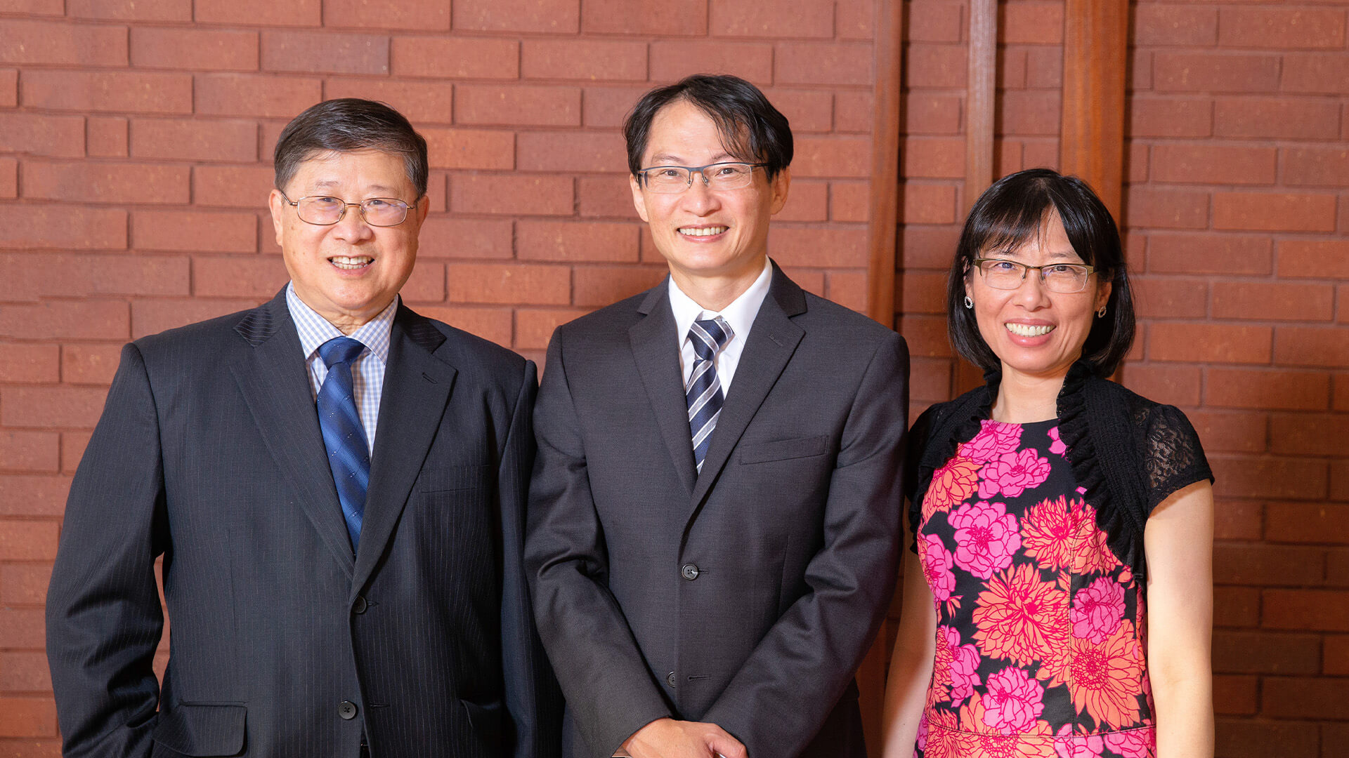
It has, of course, been dedicated to this goal from the very beginning. Having been founded in 2012 by Andy Hsu and his team in San Jose, California, the company owns more than 20 U.S. patents at present in memory design architecture and cell structure, securing its place as a household name in flash memory. Founded and led by a team of dedicated, industry-leading innovators, Andy Hsu – the CEO – takes great pride in the efficacy and incredible work of the people around him, gathering like-minded creators to his side who are equally interested in bettering the future of technology in order to improve the prospects of the global society.
Being both NEO and CEO, Andy wears many hats within the company proper. Due to his own extreme level of dedication to the cause, he uses his 25 years of experience in the semiconductor industry proper to ensure that every innovation released to the public and professional semiconductor market segment is the best that it could possibly be. Before founding NEO SEMICONDUCTOR as a company, he led the R&D and engineering teams of a start-up company for 16 years, developing more than 60 products in NOR flash, EEPROM, and NVSRAM that have become renowned as extraordinary achievements and innovations in their own right.
Fundamentally, Andy’s leadership of the company comes from a deep place of understanding regarding how the wider industry works, both as a market segment and as a place of pushing towards a brighter future for all. Over his time in the sector, he has consistently been working at the top of his game in order to push for the betterment of technology in the macro scale in this way, and today can proudly say that he is the inventor of over 100 granted US patents in the non-volatile memory area. Having earned an MS in Electrical, Computer, and System Engineering from the Rensselaer Polytechnic Institute (RPI) and a BS from the National Cheung-Kung University in Taiwan, his beginnings in making a name for himself began all the way back with his thesis in Artificial Neural Networks that he penned during Graduate School.
Andy is backed up by Ray Tsay, the Co-Founder and VP of Engineering for NEO SEMICONDUCTOR. With over 30 years of experience under his belt in the semiconductor industry and boasting a wide depth and breadth of knowledge regarding the companies that occupy the sector, his current expertise has been built up through working in many different corporate positions for many different organisations such as Silicon Solution, ICT, and EG&G Reticon. Having led teams in charge of testing, product development, and product manufacture, he has cultivated a truly incomparable understanding of the market, the customers, and the competition that currently make up the dynamic ecosystem of the semiconductor industry. Additionally, it was in these positions that he built up his current outstanding level of knowledge in various products from CCD to CPLD, as well as SRAM, EEPROM, EPROM, and Flash Memory. Ray, holding an MS degree in Electrical and Computer Engineering from Arizona State University, an MS in Chemical and Material Engineering from the University of Iowa, and a BS in Chemical Engineering from the National Central University of Taiwan, is a critical pillar in NEO SEMICONDUCTOR’s structure, and his work has been invaluable in making the firm what it is today.
For business enquiries, contact Andy Hsu from NEO SEMICONDUCTOR via their website neosemic.com